Layout Design in VLSI
In Very Large-Scale Integration (VLSI), layout design refers to the process of creating a physical representation of an integrated circuit (IC) design. It involves translating the logical circuit description from the schematic into geometric shapes and patterns that define the actual layout of transistors, interconnections, and other components on the semiconductor substrate.
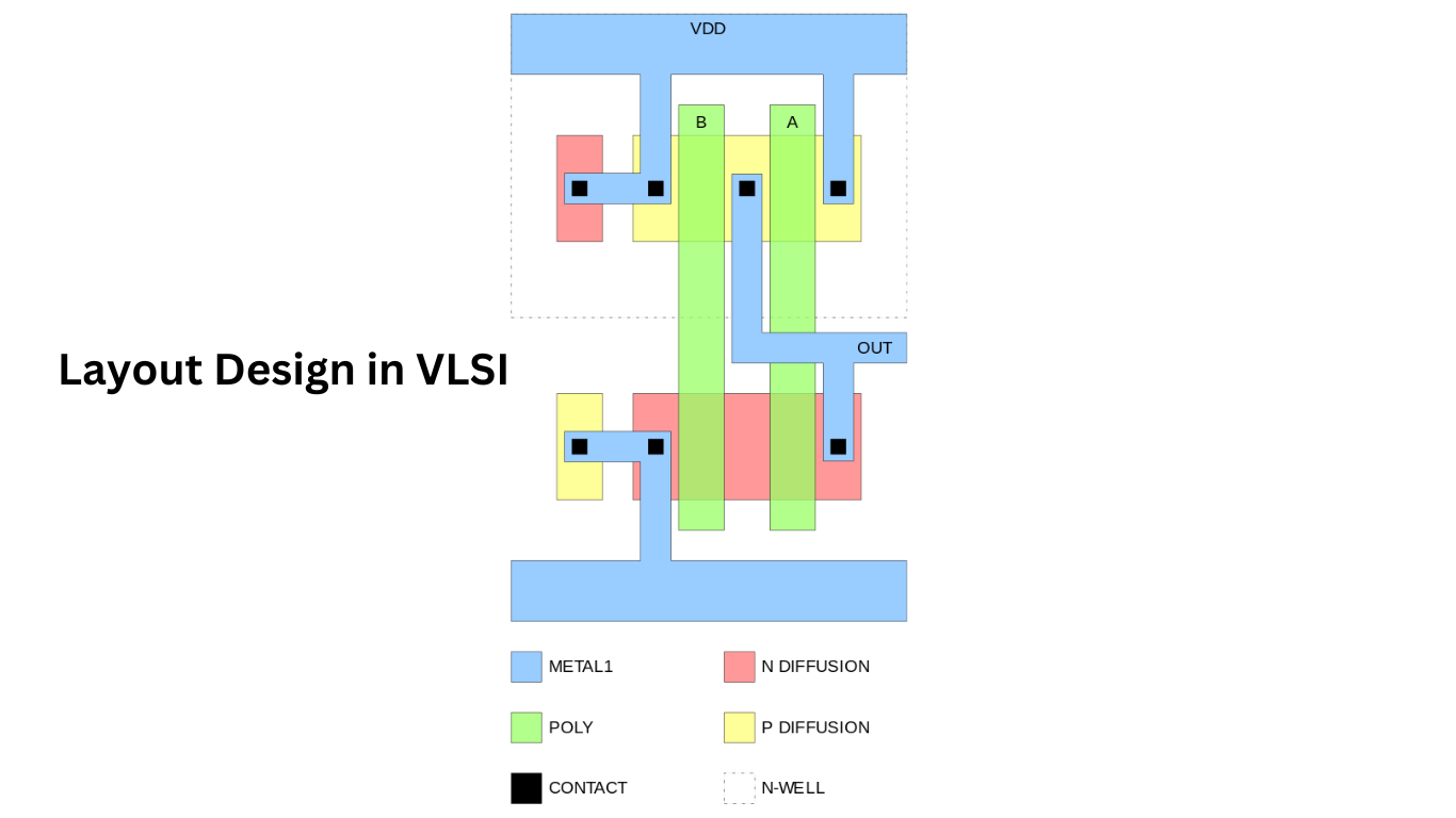
Key aspects of layout design in VLSI include:
Read also: Top 10 Analog Layout Interview Questions(2024)
- Transistor Placement: Positioning transistors and other components on the semiconductor substrate according to the specified logic functions and timing requirements.
- Routing: Creating interconnections between transistors and components to establish the desired electrical connections and signal paths while adhering to design rules and constraints.
- Physical Design Rules: Ensuring that the layout adheres to manufacturing constraints, such as minimum feature sizes, spacing requirements, and layer stack-ups, to enable successful fabrication of the IC.
- Physical Verification: Performing checks and analyses to verify the correctness and manufacturability of the layout, including design rule checking (DRC), layout versus schematic (LVS) verification, and parasitic extraction.
- Design for Manufacturability (DFM): Optimizing the layout to enhance yield, performance, and reliability during the manufacturing process, considering factors such as process variability, lithography limitations, and device parasitics.
- Power and Signal Integrity: Addressing issues related to power distribution, signal integrity, and electromagnetic interference (EMI) to ensure proper functioning and reliability of the integrated circuit.
Overall, layout design in VLSI plays a critical role in translating the abstract logical design into a physical form that can be fabricated and manufactured into functioning semiconductor chips. It requires expertise in semiconductor technology, CAD tools, design methodologies, and an understanding of the underlying physics and principles of integrated circuit design.
Related Posts
Memory Design Interview Questions
Physical Design Interview Questions
STA Interview Questions
Verilog Interview Questions
If VDD and VSS are shorted. What type of errors you will get?