Antenna Prevention Techniques in VLSI
Several techniques are used to mitigate antenna violations:
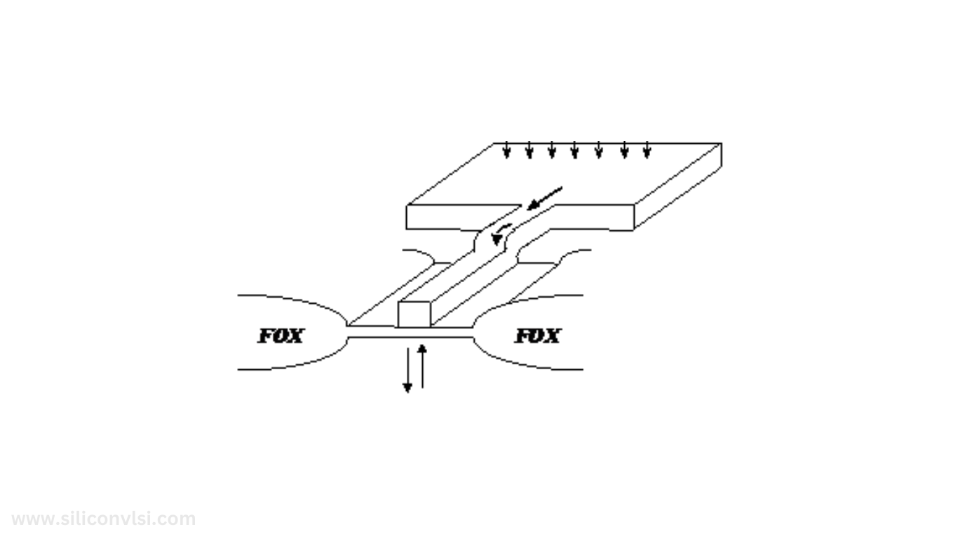
Diodes: Placing diodes near the gate can help dissipate the accumulated charge, preventing it from discharging through the gate oxide.
Metal Jumper Insertion: Introducing additional metal layers or connections to provide alternate paths for charge dissipation.
Dummy Metal Fill: Adding dummy metal structures to balance the charge accumulation.
Layer Hopping: Splitting long interconnects across multiple metal layers to reduce the effective antenna area.
Design Rule Checks (DRC): Using EDA (Electronic Design Automation) tools to check for potential antenna violations during the design phase and adjust the layout accordingly.
By understanding and addressing these factors during the design and fabrication process, antenna violations can be minimized, ensuring the reliability and performance of the integrated circuit.
Read also : VLSI Design Questions with Answers (2024)